University of California, Irvine
EECS 170C
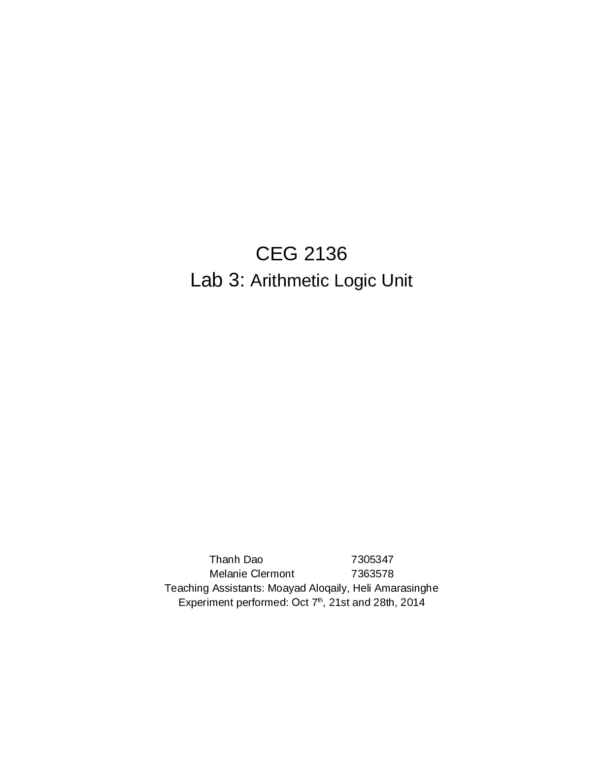
EECS 170LC 8/26/2022 Lab 2: Simulation Assignment [Sim1.] (a) In the first simulation, we are to plot the Voltage Transfer Characteristics of the commoncollector circuit shown in the figure below: Figure 1.1: Common-collector circuit Running a DC sweep from 0 to 3.3V in 10 mV step and plotting Vout vs Vin yields the figure 1.2: Figur
...[Show More]
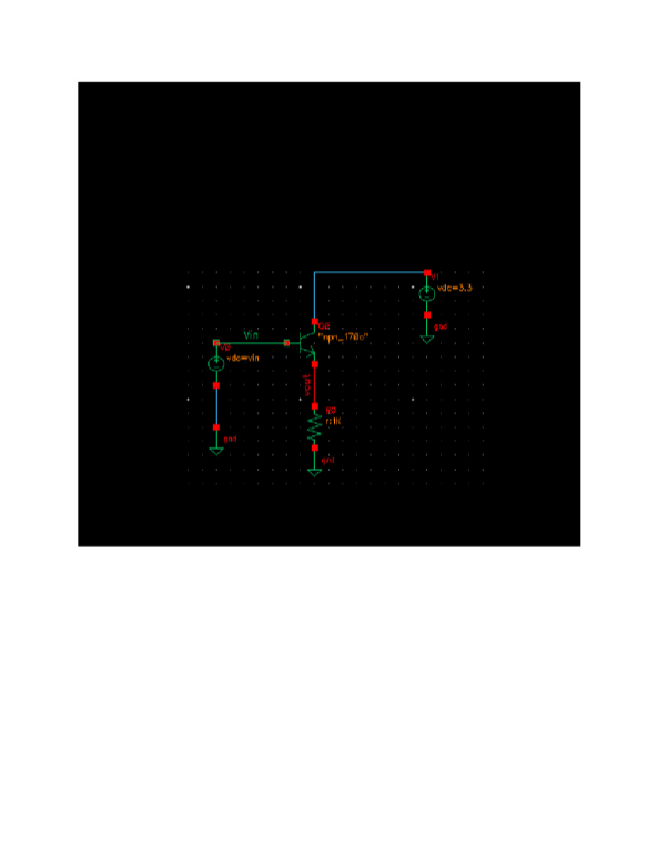
EECS 170LC 8/26/2022 Lab 2: Simulation Assignment [Sim1.] (a) In the first simulation, we are to plot the Voltage Transfer Characteristics of the commoncollector circuit shown in the figure below: Figure 1.1: Common-collector circuit Running a DC sweep from 0 to 3.3V in 10 mV step and plotting Vout vs Vin yields the figure 1.2: Figure 1.2: VTC for common-collectorcircuit As soon as the transistor turns on, the collector-emitter voltage VCE is 3.3-0.74 V or 2.56 V, which is much larger than VCE(sat), typically 0.2 ~ 0.3 V. Thus the linear region after Vin exceeds VBE(on) is when the transistor is in forward active region. The center of forward active region is approximately Vin(eq1) = 2.02 V (b) Next, I set Vin to Vin(eq1) and ran a DC operating point analysis. The following DC voltages and currents are shown in figure 1.3:
[Show Less]
-preview.png)